Sample Preparation For Electronics & Semiconductor
PRODUCTS
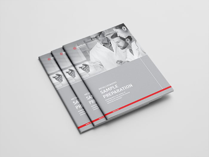
SAMPLE PREPARATION FOR ELECTRONICS & SEMICONDUCTOR
Electronics & semiconductor samples can be grouped in four different groups: Silicon wafer, chip based components, electronic components and printed circuit boards (PCB). The metallographic inspection is done usually on chip based components and electronics components for inspecting cavities, cracks, soldering errors, conductive layers etc. The structrure of chip based and electronics components are very small, which require very high precise sample preparation equipment.
ACCURA 102
MICRADEPTH
MICRACUT 200-S
SAMPLE PREPARATION FOR ELECTRONICS & SEMICONDUCTOR
The goal of sample preparation is to make visible hidden layers inside the sample or reveal interested inspection area. This can be done with precise grinding. If inspection area is at very deep from the sample edge, in this case cutting method can be used for reduce total grinding depth. After cutting and grinding, the next step is polishing. After polishing, the scratches are removed and the microstructure can be seen under microscope clearly. Metkon provides special sample preparation solution for electronic components and semiconductors.
High-quality consumables are essential for achieving consistent and accurate sample preparation results. Metkon provides a comprehensive range of cutting discs, mounting resins, grinding papers, polishing cloths, and other essential accessories. Our consumables are designed for durability and performance, ensuring optimal results in material testing and preparation processes.
LABORATORY SUPPORT
Our expert laboratory engineers and application specialists are ready to help you. We offer demonstration of our equipment and consumables and to help our customers with the perfect preparation methods for their specific samples.
Get a hands-on training tailored to enhance your team’s capabilities. Explore the full potential of our expertise with dedicated, customer-focused solutions! CONTACT OUR TEAM
SERVICE SUPPORT
At Metkon, we provide comprehensive technical support and services to ensure your equipment operates at maximum efficiency. From machine repairs and software/technical support to scheduled maintenance and calibrations, we guarantee uninterrupted performance. Additionally, with our spare parts supply and training programs, we help extend the lifespan and reliability of your equipment. Metkon’s expert technical team is always here for you!
CONTACT OUR TEAM
WHAT OUR CUSTOMERS SAY ABOUT METKON
Lorem ipsum dolor
Name Surname
Lorem ipsum dolor sit amet, consectetur adipiscing elit. Praesent in sem bibendum, tristique dolor vel, vestibulum elit. Hac habitasse Platea dictumst'ta. Cras volutpat Lorem ipsum dolor sit amet, consectetur adipiscing elit. Praesent in sem bibendum, tristique dolor vel, vestibulum elit.
We provide comprehensive resources on metallographic analysis and material science. Explore topics ranging from sample preparation techniques to microscopic examinations.